
4.3 Conventional approaches used to boost the efficiency in crystalline silicon solar PV industry
The foremost challenge in the crystalline silicon solar PV industry is to cheapen solar electricity. Manufacturers try to tackle this challenge by improving the efficiency and cutting down the module price.
One obvious approach to slash the cost of solar PV electricity is minimizing the number of light photons that escape from the cell without participating in the generation of electricity. We have already discussed two such strategies. Back reflector is another approach used to improve the efficiency by enhancing the internal reflectivity and promoting light trapping inside the cells.
Back reflector
The idea of back reflector is not new at all…
Crystalline silicon absorbs light and generates electron-hole pairs when light hits and shines on it. Electron-hole pairs then get separated leading to a photocurrent in a case of a short circuit and open-circuit voltage in a case of an open circuit. However, photons with energy less than 1.12 eV (bandgap of silicon) are not absorbed by the valance electrons as the valance electrons of silicon atoms need at least 1.12 eV of energy to jump on to its conduction band. As such, low-energy photons cannot generate electron-hole pairs. They just go through the lattice and escape.
What does it theoretically mean?
1.12 eV is equivalent to the energy of light photons whose wavelength is approximately 1100 nm. This implies that the photons with wavelengths longer than 1100 nm do not generate electron-hole pairs or a photocurrent in a cell. Further, it is worth noting that silicon is, of course, an excellent material for mass production of solar panels but it is not good at absorbing light or promoting its valance electrons to its conduction band since silicon is an indirect bandgap semiconductor material. Photon absorption and subsequent electron transition to the conduction band must, therefore, be assisted by phonons (discrete unit of vibrational energy in the lattice). Owing to this discouraging requirement, silicon atoms in the lattice miss a significant number of near-infrared light photons. These low-energy photons go through the cell and leave without getting absorbed. In particular, it has been observed that the penetration depth of the photons whose wavelengths range between 900-1100 nm is up to 3 mm whereas the typical thickness of silicon solar cells is about 180 µm! [1]
See the gap!
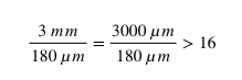
What does it imply?
The thickness of silicon wafers needs to be at least 16 times that of the wafers used in conventional solar cells in order to optimize the absorption of near-infrared light.
A puzzle
Inefficient light absorption has been one of the major barriers that hinder the development of efficient, low-cost solar PVs. In order to enhance the light absorption and efficiency, we need to use thick silicon wafers. Technology can endure the use of thick wafers but not the economy!
As we discussed in the previous articles, silicon wafers still account for about one half (51%) of the total cell price [2]. The thicker the wafer the greater the fabrication cost!
- On the one hand silicon solar cells need thick wafers for efficient absorption of light, but on the other hand, they need to be fabricated with less amount of silicon or thin silicon wafers in order to cut the fabrication cost.
Two opposite requirements!
How to succeed in?
Even though fabrication cost falls with the decreasing wafer thickness, light absorption steadily drops with the decreasing wafer thickness. A wise way to address this complicated issue is to promote the light absorption capacity while keeping the wafer thickness at an affordable level.
Light absorption can be improved by employing some light management mechanisms that improve the internal reflection, minimize the rear side’s absorption, and enhance the light trapping capacity inside the cell. That is the idea of a back reflector. Light that is not absorbed by the cell reaches the back reflector and get reflected back. This increases the chance of unabsorbed photons getting absorbed by valance electrons leading to an increase in the photocurrent. Especially, when back reflector joins with the textured front surface, it forms an excellent light trapping scheme in which previously unabsorbed photons bounce back and forth between the back reflector and textured front surface [3]. Most of the unabsorbed photons bounce back and forth several times until they get absorbed by an electron. This notably extends the optical path length of the cell while keeping the geometric length of the cell the same. In other words, the light trapping schemes virtually widen the wafer thickness which is the most expensive component of a typical solar cell. An excellent model to lift the conversion efficiency whilst cutting the amount of crystalline silicon and the fabrication cost!
Back contact & back reflector
Screen printed silver and aluminium paste is still being widely used as the rear side metallization technique to create back contact in the solar PV industry. The screen-printed paste is then fired to obtain the back surface field passivation (BSF). The back contact adds structural strength, seals off rear side of the cell and act as a conductor. Not only that but also it acts as a back reflector and closely work with the textured front surface to trap light inside. But any technology has its own limits and restrictions. It is a universal rule. Al-BSF technology has also a technical limit in improving efficiency. The tireless effort to find more-efficient alternatives to the Al-BSF technology has given rise a wide range of new solar PV species with higher efficiencies. PERC is one of the best alternatives to Al-BSF technology. It has already been able to commercialize with an efficiency enhancement of about 1% thanks to its superior performance.
Future
Today, BSF technology leads the solar PV market with the highest market share. However, its share would probably drop to about 50% by 2020 and would be less than 10% by 2028 as per recent estimations. This would be largely due to the increasing penetration of more-efficient new PV technologies such as PERC, PERL, and PERT into the PV market. [4] In addition, HIT and back contact solar PV technologies seem to be another efficient PV technologies competing in the market. All these technologies would finally, offer increasingly improved efficiency while cutting down the wafer thickness and the module price making the solar PV the most affordable energy technology.
Reference
[1] Eisenlohr, J., Benick, J., Peters, M., Bläsi, B., Goldschmidt, J. C., & Hermle, M. (2014). Hexagonal sphere gratings for enhanced light trapping in crystalline silicon solar cells. Optics express, 22 (101), A111-A119.
[2] Solanki, C. S., & Singh, H. K. (2017). Anti-reflection and Light Trapping in c-Si Solar Cells. Springer.
[3] Blakers, A. W., Wang, A., Milne, A. M., Zhao, J., & Green, M. A. (1989). 22.8% efficient silicon solar cell. Applied Physics Letters, 55 (13), 1363-1365.
[4] Fischer, M., Cells, H, Q. (2018). Trends & challenges in c-Si PV-an update of the ITRPV 9th edition. World solar congress-Shanghai.


Recent Comments